- 您现在的位置:买卖IC网 > Sheet目录1997 > ICS843001AGI-22LFT (IDT, Integrated Device Technology Inc)IC SYNTHESIZER LVPECL 24-TSSOP
ICS843001AGI-22 REVISION B JUNE 25, 2009
2
2009 Integrated Device Technology, Inc.
ICS843001I-22 Data Sheet
FEMTOCLOCK CRYSTAL/LVCMOS-TO-3.3V, 2.5V LVPECL FREQUENCY SYNTHESIZER
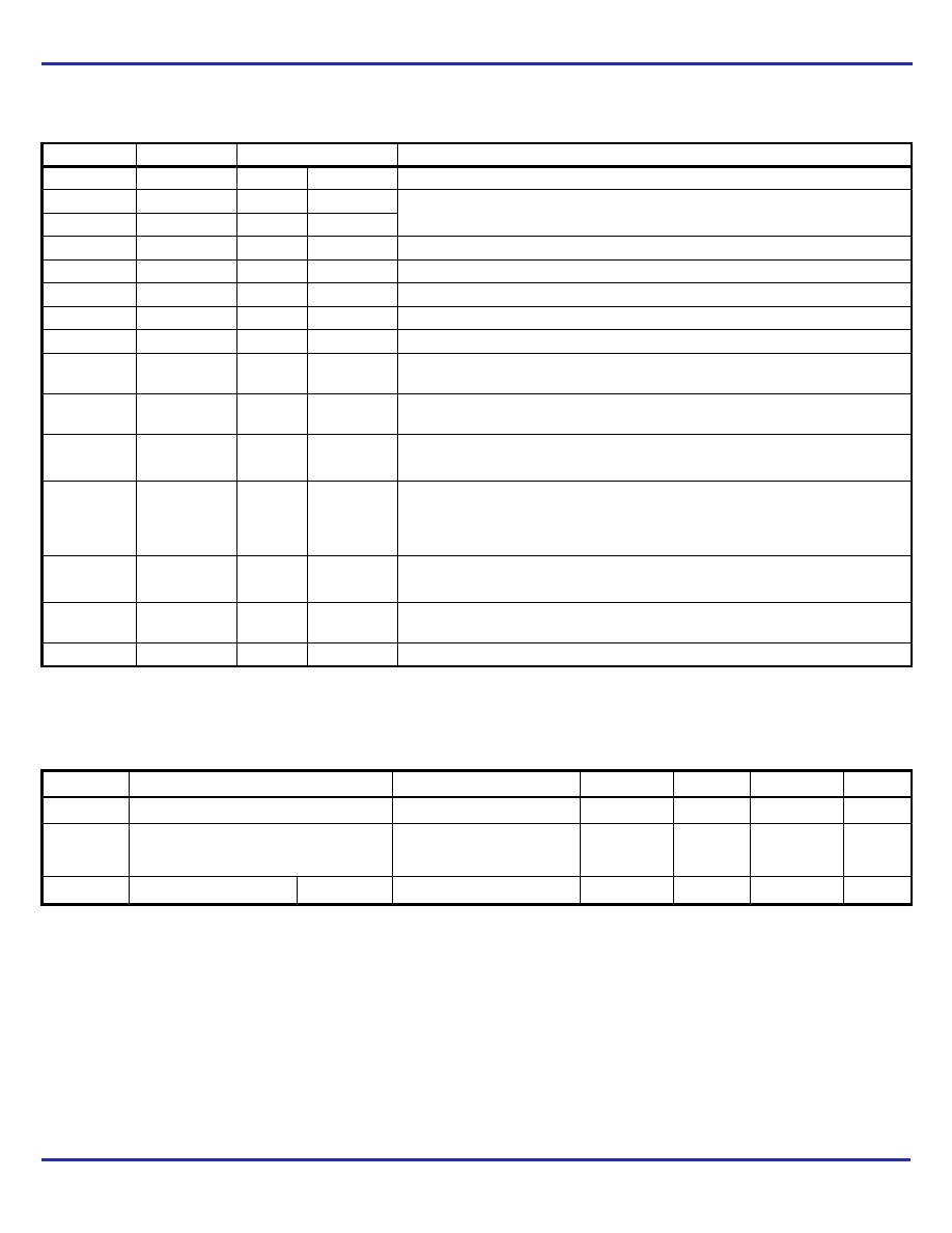
Table 1. Pin Descriptions
NOTE: Pullup and Pulldown refer to internal input resistors. See Table 2, Pin Characteristics, for typical values.
Table 2. Pin Characteristics
Number
Name
Type
Description
1VCCO_LVCMOS
Power
Output supply pin for REF_CLK output.
2, 3
N0, N1
Input
Pullup
Output divider select pins. Default ÷4. LVCMOS/LVTTL interface levels.
See Table 3C.
4
N2
Input
Pulldown
5VCCO_LVPECL
Power
Output supply pin for LVPECL output.
6, 7
Q, nQ
Output
Differential output pair. LVPECL interface levels.
8, 23
VEE
Power
Negative supply pins.
9VCCA
Power
Analog supply pin.
10
VCC
Power
Core supply pin.
11,
12
XTAL_OUT1,
XTAL_IN1
Input
Parallel resonant crystal interface.
XTAL_OUT1 is the output, XTAL_IN1 is the input.
13,
14
XTAL_OUT0,
XTAL_IN0
Input
Parallel resonant crystal interface.
XTAL_OUT0 is the output, XTAL_IN0 is the input.
15
CLK
Input
Pulldown
LVCMOS/LVTTL clock input.
16, 17
SEL0, SEL1
Input
Pulldown
Input MUX select pins. LVCMOS/LVTTL interface levels. See Table 3D.
18
MR
Input
Pulldown
Active HIGH Master Reset. When logic HIGH, the internal dividers are reset
causing the true output Q to go low and the inverted output nQ to go high.
When logic LOW, the internal dividers and the outputs are enabled.
LVCMOS/LVTTL interface levels.
19, 20
M0, M1
Input
Pulldown
Feedback divider select pins. Default value = ÷32. See Table 3B.
LVCMOS/LVTTL interface levels.
21
M2
Input
Pullup
22
OE
Input
3-State clock output enable, (High/Low/Float). See page 1, Control Input Function
Table.
24
REF_OUT
Output
Reference clock output. LVCMOS/LVTTL interface levels.
Symbol
Parameter
Test Conditions
Minimum
Typical
Maximum
Units
CIN
Input Capacitance
4pF
RPULLUP
Input Pullup Resistor
51
k
RPULLDOWN Input Pulldown Resistor
51
k
ROUT
Output Impedance
REF_OUT
15
发布紧急采购,3分钟左右您将得到回复。
相关PDF资料
ICS843001AKI-40LF
IC SYNTHESIZER LVPECL 16-VFQFPN
ICS843002AGI-01LF
IC SYNTHESIZER LVPECL 20-TSSOP
ICS843002AKI-41LF
IC SYNTHESIZER LVPECL 32-VFQFPN
ICS843004AG-02LF
IC SYNTHESIZER LVPECL 24-TSSOP
ICS843004AGI-04LF
IC SYNTHESIZER LVPECL 24-TSSOP
ICS843021AGLFT
IC CLK GENERATOR LVPECL 8-TSSOP
ICS843022AGLF
IC CLK GENERATOR LVPECL 8-TSSOP
ICS843023AGLF
IC CLK GENERATOR LVPECL 8-TSSOP
相关代理商/技术参数
ICS843001AGI-22T
制造商:ICS 制造商全称:ICS 功能描述:FEMTOCLOCKS? CRYSTAL/LVCMOS-TO-3.3V, 2.5V LVPECL FREQUENCY SYNTHESIZER
ICS843001AGI-23
制造商:ICS 制造商全称:ICS 功能描述:FEMTOCLOCKS⑩ CRYSTAL-TO-3.3V LVPECL/LVCMOS FREQUENCY SYNTHESIZER
ICS843001AGI-23LF
功能描述:IC SYNTHESIZER LVPECL 24-TSSOP RoHS:是 类别:集成电路 (IC) >> 时钟/计时 - 时钟发生器,PLL,频率合成器 系列:HiPerClockS™, FemtoClock™ 标准包装:27 系列:Precision Edge® 类型:频率合成器 PLL:是 输入:PECL,晶体 输出:PECL 电路数:1 比率 - 输入:输出:1:1 差分 - 输入:输出:无/是 频率 - 最大:800MHz 除法器/乘法器:是/无 电源电压:3.135 V ~ 5.25 V 工作温度:0°C ~ 85°C 安装类型:表面贴装 封装/外壳:28-SOIC(0.295",7.50mm 宽) 供应商设备封装:28-SOIC 包装:管件
ICS843001AGI-23LFT
功能描述:IC SYNTHESIZER LVPECL 24-TSSOP RoHS:是 类别:集成电路 (IC) >> 时钟/计时 - 时钟发生器,PLL,频率合成器 系列:HiPerClockS™, FemtoClock™ 标准包装:27 系列:Precision Edge® 类型:频率合成器 PLL:是 输入:PECL,晶体 输出:PECL 电路数:1 比率 - 输入:输出:1:1 差分 - 输入:输出:无/是 频率 - 最大:800MHz 除法器/乘法器:是/无 电源电压:3.135 V ~ 5.25 V 工作温度:0°C ~ 85°C 安装类型:表面贴装 封装/外壳:28-SOIC(0.295",7.50mm 宽) 供应商设备封装:28-SOIC 包装:管件
ICS843001AGI-23T
制造商:ICS 制造商全称:ICS 功能描述:FEMTOCLOCKS⑩ CRYSTAL-TO-3.3V LVPECL/LVCMOS FREQUENCY SYNTHESIZER
ICS843001AGLF
功能描述:IC CLK GEN FIBRE LVPECL 8-TSSOP RoHS:是 类别:集成电路 (IC) >> 时钟/计时 - 时钟发生器,PLL,频率合成器 系列:HiPerClockS™, FemtoClock™ 标准包装:2,000 系列:- 类型:PLL 频率合成器 PLL:是 输入:晶体 输出:时钟 电路数:1 比率 - 输入:输出:1:1 差分 - 输入:输出:无/无 频率 - 最大:1GHz 除法器/乘法器:是/无 电源电压:4.5 V ~ 5.5 V 工作温度:-20°C ~ 85°C 安装类型:表面贴装 封装/外壳:16-LSSOP(0.175",4.40mm 宽) 供应商设备封装:16-SSOP 包装:带卷 (TR) 其它名称:NJW1504V-TE1-NDNJW1504V-TE1TR
ICS843001AGLFT
功能描述:IC CLOCK GENERATOR 8-TSSOP RoHS:是 类别:集成电路 (IC) >> 时钟/计时 - 时钟发生器,PLL,频率合成器 系列:HiPerClockS™, FemtoClock™ 标准包装:1,000 系列:- 类型:时钟/频率合成器,扇出分配 PLL:- 输入:- 输出:- 电路数:- 比率 - 输入:输出:- 差分 - 输入:输出:- 频率 - 最大:- 除法器/乘法器:- 电源电压:- 工作温度:- 安装类型:表面贴装 封装/外壳:56-VFQFN 裸露焊盘 供应商设备封装:56-VFQFP-EP(8x8) 包装:带卷 (TR) 其它名称:844S012AKI-01LFT
ICS843001AGT
制造商:ICS 制造商全称:ICS 功能描述:FEMTO CLOCKS CRYSTAL-TO- 3.3V LVPECL CLOCK GENERATOR